- Автоматизация
- Антропология
- Археология
- Архитектура
- Биология
- Ботаника
- Бухгалтерия
- Военная наука
- Генетика
- География
- Геология
- Демография
- Деревообработка
- Журналистика
- Зоология
- Изобретательство
- Информатика
- Искусство
- История
- Кинематография
- Компьютеризация
- Косметика
- Кулинария
- Культура
- Лексикология
- Лингвистика
- Литература
- Логика
- Маркетинг
- Математика
- Материаловедение
- Медицина
- Менеджмент
- Металлургия
- Метрология
- Механика
- Музыка
- Науковедение
- Образование
- Охрана Труда
- Педагогика
- Полиграфия
- Политология
- Право
- Предпринимательство
- Приборостроение
- Программирование
- Производство
- Промышленность
- Психология
- Радиосвязь
- Религия
- Риторика
- Социология
- Спорт
- Стандартизация
- Статистика
- Строительство
- Технологии
- Торговля
- Транспорт
- Фармакология
- Физика
- Физиология
- Философия
- Финансы
- Химия
- Хозяйство
- Черчение
- Экология
- Экономика
- Электроника
- Электротехника
- Энергетика
product picture. Hardware structure. Digital to analog conversion (DA) circuit

High speed AD/DA moduleuser's guidance Rev 1.3

一、 product picture
 二、 Acknowledgement
Thank you for purchasing the high-speed AD/DA module from the Black Gold Power Community. This module needs to be used with other development boards to temporarily support the FPGA Black Gold Development Board (DB2C8) and the FPGA Black Gold Development Board Student Edition (DB2C5). Updated through the Black Gold Power Community.
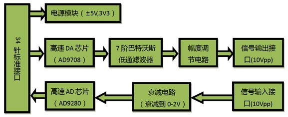
三、 Hardware structure
四、 Digital to analog conversion (DA) circuit
As shown in the hardware structure diagram, the DA circuit consists of a high-speed DA chip, a 7th-order Butterworth low-pass filter, a amplitude adjustment circuit, and a signal output interface.
The high-speed DA chip we use is the AD9708 from AD. The AD9708 is an 8-bit, 125MSPS DA conversion chip with a built-in 1.2V reference and differential current output. The internal structure of the chip is shown in the figure below.

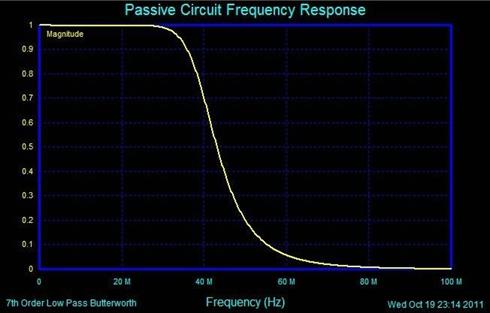
After the differential output of the AD9708 chip, in order to prevent noise interference, a 7th-order Butterworth low-pass filter is connected to the circuit with a bandwidth of 40MHz. The frequency response is shown in the figure below.
The filter parameters are shown below 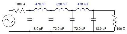
After the filter, we used two high-performance 145MHz bandwidth op amp AD8056 to achieve differential single-ended, amplitude adjustment and other functions, so that the entire circuit performance is maximized. The amplitude is adjusted using a 5K potentiometer and the final output range is -5V to 5V (10Vpp).
|
|
|
© helpiks.su При использовании или копировании материалов прямая ссылка на сайт обязательна.
|